Call us now :08045812175
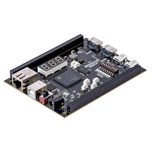
Skoll K7 USB Ready To Go FPGA Module
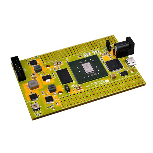

Skoll K7 USB Ready To Go FPGA Module Specification
- Test
- 100% E-test
- Flame Resistance Level
- UL94 V-0
- Silkscreen
- White
- Impedance
- Controlled, 50 Ohm
- Board Type
- SMD/DIP Mixed
- Soldermask
- Green
- Hole Size
- 0.3 mm (min)
- Min. Line Width
- 0.152 mm (6 mil)
- Min. Line Spacing
- 0.152 mm (6 mil)
- Voltage Endurance
- 250 V AC
- Insulation Resistance
- >10^8
- Product Type
- FPGA Development board
- Base Material
- FR4
- Surface Finish
- ENIG (Electroless Nickel/Immersion Gold)
- Copper Thickness
- 35 m
- Board Thickness
- 1.6 mm
- Color
- Green
- Sensor Switch
- No
- Electrical Components
- FPGA, USB Connector, Voltage Regulators, Oscillator
- Number Of Layers
- 4 Layers
- Power Supply
- USB powered or external 5V DC
- Onboard LEDs
- User programmable, Power status indicator
- Clock Source
- 100 MHz onboard oscillator
- Dimensions
- Approx. 120 mm x 80 mm
- Memory
- DDR3 1 GB
- USB Interface
- Micro USB (USB 2.0, JTAG & UART support)
- RoHS Compliant
- Yes
- Programming Support
- JTAG, Micro USB
- Operating Temperature
- 0C to 70C
- I/O Pins
- Over 150 user I/O pins, multiple FMC/HPC connectors
- Supported Tools
- Xilinx Vivado, ISE Design Suite
- FPGA Chip
- Xilinx Kintex-7 (XC7K325T-2FFG676C)
Skoll K7 USB Ready To Go FPGA Module Trade Information
- Minimum Order Quantity
- 1 Unit
- Supply Ability
- 10 Units Per Day
- Delivery Time
- 1-4 Days
About Skoll K7 USB Ready To Go FPGA Module
Features
- FPGA: AMD XC7K70T in FBG484 package, Speed Grade: 1
- DDR3: 2Gb DDR3 (MT41J128M16HA-125:K)
- Flash memory: 128 Mb Quad bit SPI flash memory (N25Q128A13EF840E)
- 100MHz CMOS oscillator
- High-Speed USB 2.0 interface for On-board flash programming. FT2232H Channel A is dedicated to SPI Flash /JTAG Programming. Channel B can be used for custom applications.
- Onboard voltage regulators for single power rail operation
- FPGA configuration via JTAG and USB
- Maximum IOs for user-defined purposes
- FPGA 150 IOs, FT2232H 8 IOs
Applications
- Product Prototype Development
- Accelerated computing integration
- Development and testing of custom embedded processors
- Signal Processing
- Communication device development
- Educational tool for Schools and Universities
High-Performance Kintex-7 FPGA Platform
Harness the computational power and versatility of the Xilinx Kintex-7 FPGA, supported by 1 GB DDR3 memory and over 150 user I/O pins for multitasking and rich connectivity. The Skoll K7's multiple FMC/HPC connectors support a range of high-speed peripherals, making this module a robust solution for demanding industrial and academic applications.
Robust Design and Easy Integration
Crafted with a 4-layer FR4 PCB, ENIG surface finish, and controlled impedance, the Skoll K7 ensures signal integrity and longevity. Ready for integration, it features convenient programming via JTAG or Micro USB, and can be powered through USB or an external 5V DC source for versatility in lab and field environments.
Comprehensive Tool Support and Ease of Use
The module is supported by Xilinx Vivado and ISE Design Suite, offering seamless development and debugging. Its status and programmable LEDs simplify user interaction, while plug-and-play USB interface (with JTAG and UART) streamlines setup and programming. The Skoll K7 delivers everything needed for a streamlined FPGA development workflow.
FAQ's of Skoll K7 USB Ready To Go FPGA Module:
Q: How can I program the Skoll K7 FPGA module?
A: You can program the Skoll K7 module using either the onboard Micro USB port (supporting JTAG) or a dedicated JTAG interface. Tools such as Xilinx Vivado or the ISE Design Suite are fully compatible with this device, enabling easy configuration and debugging.Q: What are the primary benefits of the Skoll K7 module for developers?
A: The Skoll K7 offers a high-performance Kintex-7 FPGA, over 150 user I/O pins, and extensive FMC/HPC connectivity, making it ideal for rapid prototyping and complex design implementations. Its user-friendly interfaces, robust PCB design, and comprehensive tool compatibility benefit both academic and industrial users.Q: Where is the Skoll K7 module most commonly used?
A: This module is used extensively in research institutions, universities, and industries focusing on signal processing, embedded systems, high-speed data acquisition, and real-time application development where flexible FPGA platforms are essential.Q: What is the process for powering and getting started with the module?
A: Simply connect the Skoll K7 to your computer using the Micro USB port for both power and communication, or use an external 5V DC adapter if additional power is required. Once connected, use Vivado or ISE Design Suite to initialize your designs and begin development.Q: When should I consider using an external 5V DC supply instead of USB power?
A: An external 5V DC supply is recommended when your application draws significant current, such as when multiple peripherals are connected or when driving a large number of I/O. For lighter or prototyping tasks, USB power is often sufficient.Q: How do the onboard LEDs and status indicators assist in module usage?
A: The user-programmable LEDs allow developers to quickly visualize the status of their designs or debugging processes. The power status indicator provides immediate confirmation that the board is receiving power and operating within the specified range.Q: What compliance and safety features does the Skoll K7 offer?
A: The module is RoHS compliant, tested for electrical reliability (including UL94 V-0 flame resistance), and passes 100% E-test quality checks. Such measures ensure both safety and consistent operational standards for users.Tell us about your requirement

Price:
Quantity
Select Unit
- 50
- 100
- 200
- 250
- 500
- 1000+
Additional detail
Mobile number
Email

More Products in FPGA Boards Category
Callisto K7 USB 3.1 FPGA Module
Price 229.0 INR / Unit
Minimum Order Quantity : 1 Unit
Product Type : FPGA Development board
Board Type : Rigid
Base Material : Other, FR4
Board Thickness : 1.6 mm
Mimas V2 S6 FPGA Development Board with DDR SDRAM
Price 7150 INR / Unit
Minimum Order Quantity : 1 Unit
Product Type : FPGA Development board
Board Type : Other, SMD and TH Components
Base Material : FR4
Board Thickness : 1.6 mm
FPGA Board
Price 160.0 INR / Unit
Minimum Order Quantity : 1 Unit
Product Type : FPGA Development board
Board Type : Rigid
Base Material : FR4
Board Thickness : 1.6 mm
FPGA Development Board
Price 70.0 INR / Unit
Minimum Order Quantity : 1 Unit
Product Type : FPGA Development board
Board Type : Other, FR4 PCB
Base Material : Other
Board Thickness : 1.6 mm
Our Products


H No 2-3-54, Co-Operative Bank Colony, Road No. 6, Nogole,Hyderabad - 500068, Telangana, India

Mr Suneel
Mobile :08045812175
 Send Inquiry
 Send SMS
 Call Me Free
Developed and Managed by Infocom Network Private Limited.
