Call us now :08045812175
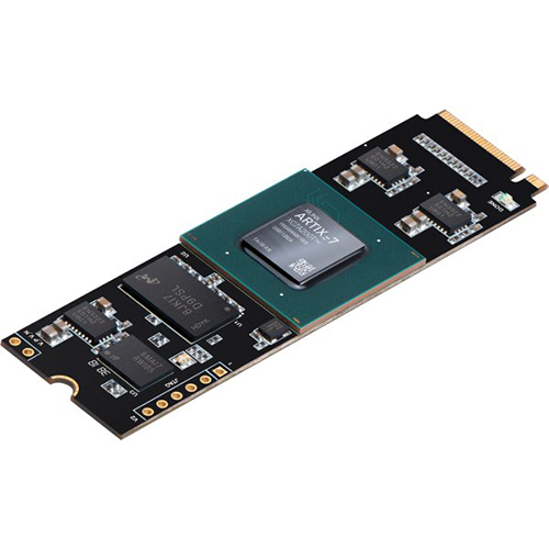
Callisto K7 USB 3.1 FPGA Module
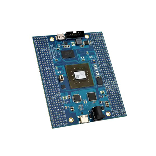

Callisto K7 USB 3.1 FPGA Module Specification
- Min. Line Spacing
- 0.1 mm
- Board Type
- Rigid
- Silkscreen
- White
- Min. Line Width
- 0.1 mm
- Hole Size
- 0.3 mm (min.)
- Insulation Resistance
- >10^12
- Voltage Endurance
- >1000V
- Flame Resistance Level
- UL 94V-0
- Impedance
- Controlled impedance
- Soldermask
- Green
- Test
- 100% E-Test
- Product Type
- FPGA Development board
- Base Material
- FR-4
- Surface Finish
- ENIG (Electroless Nickel Immersion Gold)
- Copper Thickness
- 1 oz (35um)
- Board Thickness
- 1.6 mm
- Color
- Green
- Panel Size
- Custom (per design)
- Sensor Switch
- No
- Electrical Components
- Integrated with Xilinx Kintex-7 FPGA
- Number Of Layers
- 6 Layers
- RoHS Compliance
- Yes
- Clock Sources
- 100 MHz onboard oscillator
- Dimensions
- Approx. 100mm x 60mm
- FPGA Device
- Xilinx Kintex-7 (325T)
- Programming Options
- USB-JTAG, direct configuration
- Power Supply
- 5V (USB powered)
- I/O Voltage
- 3.3V (standard)
- Target Applications
- High-speed data acquisition, prototyping, embedded computing
- USB Interface
- USB 3.1 Type-C
- User I/O Pins
- 120+ user I/Os exposed via pin connectors
- On-board RAM
- 1GB DDR3 SDRAM
- Debug Support
- JTAG header
- Operating Temperature
- 0C to +70C
- Expansion Capability
- High-speed I/O, PMOD compatible headers
- On-board Flash
- 64MB SPI Flash
Callisto K7 USB 3.1 FPGA Module Trade Information
- Minimum Order Quantity
- 1 Unit
- Supply Ability
- 10 Units Per Day
- Delivery Time
- 1-4 Days
About Callisto K7 USB 3.1 FPGA Module
Features
- FPGA: AMD XC7K160T in FBG676 package
- DDR3: 4Gb DDR3 (MT41J256M16HA-125:K or equivalent)
- Flash memory: 512 Mb Quadbit SPI flash memory (S25FL512SDSBHV210/IS25LP512M-RHLE)
- 1 x 100MHz CMOS oscillator
- USB 3.1 Gen1 @5Gbps (USB Type-C connector)
- Onboard voltage regulators for single power rail operation
- 12V DC power supply
- A Push Button for the reset pin
- JTAG header for programming and debugging
- 274 IOs for user-defined purposes
- All user IOs are length matched and can be used as differential pairs
Applications
- Product Prototype Development
- Communication Device Development
- Accelerated Computing Integration
- Development and Testing of Custom embedded processors
- Signal Processing
- Educational tool for Schools and Universities
Advanced FPGA Performance
The module integrates the Xilinx Kintex-7 (325T) FPGA, known for delivering high computational power and flexibility. This makes it well-suited for complex logic designs, digital signal processing, and applications requiring rapid data throughput, such as scientific instrumentation and embedded computing.
High-Speed USB 3.1 Interface
A native USB 3.1 Type-C interface ensures fast connectivity for data transfers and programming. Coupled with USB-JTAG support, users can quickly configure and debug their FPGA designs with modern devices, streamlining the development process and minimizing downtime.
Extensive Expansion and I/O
With over 120 user I/O pins exposed via robust connectors, and PMOD-compatible headers, the Callisto K7 offers excellent options for custom peripheral interfacing. The board also features high-speed I/O expansion, 1GB DDR3 RAM for temporary data storage, and 64MB SPI flash for non-volatile storage needs.
FAQ's of Callisto K7 USB 3.1 FPGA Module:
Q: How do I program the Callisto K7 USB 3.1 FPGA Module?
A: You can program the Callisto K7 using the USB-JTAG interface or direct configuration via the USB 3.1 Type-C port. The board supports configuration from onboard SPI Flash or through Xilinx programming tools, making setup straightforward for a wide range of development environments.Q: What benefits does the USB 3.1 Type-C interface offer for this FPGA module?
A: The USB 3.1 Type-C interface enables rapid data transfer speeds and reliable communication with host devices. It simplifies the connection, powering the board directly from the USB port, and supports high-throughput applications such as data acquisition and real-time processing.Q: Where can I use the Callisto K7 FPGA module?
A: This module is ideal for prototyping, high-speed data acquisition systems, embedded computing, and designs requiring extensive user I/O. Its robust construction and industrial temperature range make it suitable for research labs, development facilities, and educational institutions.Q: When is the onboard 1GB DDR3 SDRAM utilized?
A: The onboard 1GB DDR3 SDRAM is used during high-speed data processing or storage-intensive operations within your FPGA design. It serves as volatile memory for buffering, caching, or real-time signal processing tasks that demand fast and temporary data access.Q: What is the process for expanding the Callisto K7's I/O capabilities?
A: You can expand the Callisto K7's I/O by utilizing its more than 120 user I/O pins, high-speed connectors, and PMOD-compatible headers. These allow easy attachment of custom peripherals, sensors, or additional modules based on your project's requirements.Q: How does the Callisto K7 support debugging and development?
A: The module provides a dedicated JTAG header and supports USB-JTAG debug interfaces. This enables efficient FPGA configuration, real-time debugging, and monitoring during development, facilitating a streamlined workflow for engineers and developers.Tell us about your requirement

Price:
Quantity
Select Unit
- 50
- 100
- 200
- 250
- 500
- 1000+
Additional detail
Mobile number
Email

More Products in FPGA Boards Category
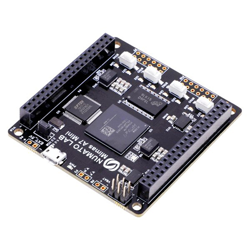
Mimas A7 Mini FPGA Development Board
Price 16500 INR / Unit
Minimum Order Quantity : 1 Unit
Voltage Endurance : 250V AC
Product Type : FPGA Development board
Test : Other, 100% Electrical Test
Sensor Switch : Tactile Push Button
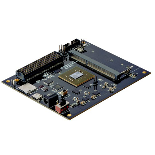
Proteus K7 USB 3.1 Development Board
Price 110000 INR / Unit
Minimum Order Quantity : 1 Unit
Voltage Endurance : >500V
Product Type : FPGA Development board
Test : Other, Etest (Professional)
Sensor Switch : Tactile Switch Onboard
Mimas A7 FPGA Development Board
Price 25300 INR / Unit
Minimum Order Quantity : 1 Unit
Voltage Endurance : 250V AC
Product Type : FPGA Development board
Test : Other, 100% Electrical Testing
Sensor Switch : Tactile Push Buttons
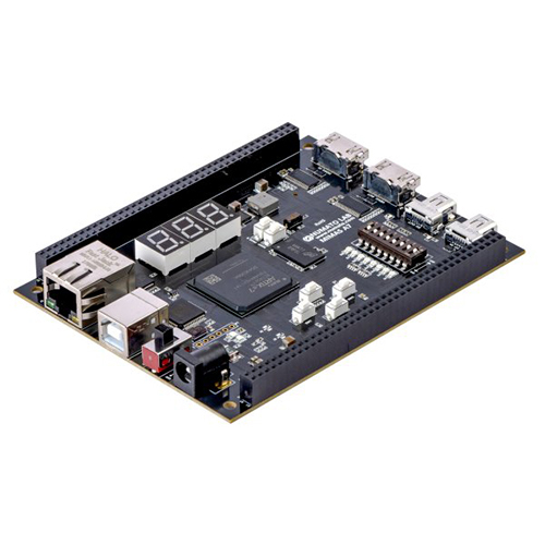
Aller A7 FPGA Board with M.2 Interface
Price 55000 INR / Unit
Minimum Order Quantity : 1 Unit
Voltage Endurance : 1000V
Product Type : FPGA Development board
Test : Other, 100% ETested
Sensor Switch : No
Our Products


H No 2-3-54, Co-Operative Bank Colony, Road No. 6, Nogole,Hyderabad - 500068, Telangana, India

Mr Suneel
Mobile :08045812175
 Send Inquiry
 Send SMS
 Call Me Free
Developed and Managed by Infocom Network Private Limited.
