Call us now :08045812175
Aller A7 FPGA Board with M.2 Interface
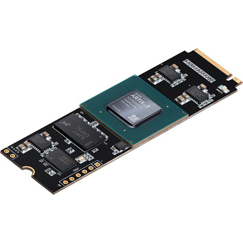

Aller A7 FPGA Board with M.2 Interface Specification
- Board Type
- Rigid
- Min. Line Spacing
- 6 mil
- Test
- 100% E-Tested
- Voltage Endurance
- 1000V
- Impedance
- Controlled Impedance
- Flame Resistance Level
- UL 94V-0
- Insulation Resistance
- >=10^12
- Min. Line Width
- 6 mil
- Soldermask
- Green
- Hole Size
- 0.3 mm min
- Silkscreen
- White
- Product Type
- FPGA Development board
- Base Material
- FR4
- Surface Finish
- ENIG (Electroless Nickel Immersion Gold)
- Copper Thickness
- 1 oz
- Board Thickness
- 1.6 mm
- Color
- Green
- Panel Size
- Standard
- Sensor Switch
- No
- Electrical Components
- Pre-soldered high-quality SMD/TH components
- Number Of Layers
- 4 Layers
- Operating Temperature
- 0C to 70C
- USB Interface
- USB 2.0 (for programming/debugging)
- Voltage Input
- 5V DC via USB-C
- Compliance
- RoHS compliant
- Mounting Holes
- 4 x M3
- Configuration
- JTAG and flash supported
- Dimensions
- Approx. 100mm x 60mm
- Expansion Headers
- Standard 2.54mm pitch
- FPGA Chip
- Xilinx Artix-7 (XC7A35T or XC7A100T Variant)
- Memory
- DDR3 SDRAM onboard
- Onboard LEDs
- Status and debug indication
- M.2 Slot
- 1x M.2 M-Key interface, PCIe Gen2 x4
- Connectivity
- Support for SYZYGY or PMOD expansion
- Clock
- Onboard 100 MHz oscillator
Aller A7 FPGA Board with M.2 Interface Trade Information
- Minimum Order Quantity
- 1 Unit
- Supply Ability
- 10 Units Per Day
- Delivery Time
- 1-4 Days
About Aller A7 FPGA Board with M.2 Interface
Features
- Device: AMD Artix 7 FPGA (XC7A200T-2FBG484I)
- DDR3: 2Gb DDR3 ( MT41J128M16JT-125:K TR )
- 4 lane PCIe Gen2 (5 GT/s)
- Flash memory: 512 Mb Quadbit SPI flash memory (S25FL512SDSBHV210/IS25LP512M-RHLE)
- JTAG header for programming and debugging
- 100 MHZ CMOS oscillator
- 1 x Trusted Platform Module (AT97SC3205)
- M.2 Connector Interface, M-Key
- Powered from M.2 connector
- 1 RGB LED for custom use
Applications
- Product Prototype Development
- Accelerated computing integration
- Development and testing of custom embedded processors
- Signal Processing
- Memory Intensive FPGA development
- Educational tool for Schools and Universities
- High Hash Rate calculations for Blockchain technologies such as Bitcoin and Ethereum
- Offloading computationally intensive algorithms to FPGA
- Machine Learning and Artificial Intelligence
Versatile FPGA Board with Powerful Connectivity
The Aller A7 FPGA Board stands out with its integration of a Xilinx Artix-7 FPGA and a high-speed M.2 interface, making it ideal for modern embedded and hardware acceleration projects. Its PCIe Gen2 x4 support, DDR3 SDRAM, and multiple expansion possibilities allow developers to scale their applications swiftly and efficiently.
Designed for Flexibility and Durability
With a compact footprint, robust mounting holes, and high-quality construction, the Aller A7 suits both rapid prototyping and deployment. Careful attention to board integrity, controlled impedance, and stringent UL 94V-0 flame rating ensure long-lasting performance across the supported temperature range.
Easy Programming and Debugging
Featuring a simple USB 2.0 interface for programming and debugging, the board makes FPGA development accessible for engineers of all proficiency levels. JTAG and flash configuration options, onboard status LEDs, and e-tested reliability streamline the development workflow and reduce setup time.
FAQ's of Aller A7 FPGA Board with M.2 Interface:
Q: How can I program and debug the Aller A7 FPGA Board?
A: You can easily program and debug the board using the USB 2.0 interface provided. The board supports both JTAG and flash configuration methods for flexible development. Onboard status and debug LEDs assist in monitoring the programming process.Q: What expansion options are supported by the Aller A7 FPGA Board?
A: The board features standard 2.54mm pitch headers and supports both SYZYGY and PMOD expansions, enabling a wide range of additional peripherals and custom daughter cards for extended functionality.Q: Where can this FPGA board be used effectively?
A: Designed for versatility, the Aller A7 suits embedded applications requiring high-speed data processing, hardware prototyping, and educational projects. Its M.2 interface and PCIe Gen2 x4 support make it particularly useful for interfacing with modern storage or acceleration modules.Q: What are the power input requirements and how is the board powered?
A: The Aller A7 requires a 5V DC input, conveniently supplied via a USB-C connection, ensuring compatibility with standard power sources and simplifying integration into various setups.Q: When is using the M.2 M-Key slot beneficial for a project?
A: Utilizing the M.2 M-Key slot is advantageous when rapid data transfer via PCIe Gen2 x4 is needed-such as for high-speed storage, real-time data acquisition, or computational offloading-leveraging the board's advanced interface capabilities.Q: What makes the Aller A7 durable and reliable for industrial or educational use?
A: The board features a robust 4-layer FR4 construction with 1 oz copper, controlled impedance, ENIG surface finish, and a flame resistance level of UL 94V-0. All boards are 100% E-tested to ensure reliable performance in demanding environments.Q: How does the onboard 100 MHz oscillator benefit FPGA development?
A: The integrated 100 MHz oscillator provides a stable and accurate clock reference, supporting a variety of timing-critical applications and enabling reliable operation of custom FPGA designs without the need for external clock sources.Tell us about your requirement

Price:
Quantity
Select Unit
- 50
- 100
- 200
- 250
- 500
- 1000+
Additional detail
Mobile number
Email

More Products in FPGA Boards Category
Callisto K7 USB 3.1 FPGA Module
Price 229.0 INR / Unit
Minimum Order Quantity : 1 Unit
Insulation Resistance : >10^12
Electrical Components : Integrated with Xilinx Kintex7 FPGA
Copper Thickness : 1 oz (35um)
Panel Size : Custom (per design)
Mimas S7 Lite
Price 11000 INR / Unit
Minimum Order Quantity : 1 Unit
Insulation Resistance : >10^12
Electrical Components : SMD and Through Hole
Copper Thickness : 35 m
Panel Size : 100 mm x 75 mm
Saturn S6 FPGA Development Board with DDR SDRAM
Price 19800 INR / Unit
Minimum Order Quantity : 1 Unit
Insulation Resistance : >10^12
Electrical Components : Xilinx Spartan6 LX45 FPGA, DDR SDRAM, USB UART, Flash Memory, FT2232H for JTAG & UART
Copper Thickness : 35m (1 oz/ft)
Panel Size : Standard 8 x 6

Callisto S6 USB 3.1 FPGA Module
Price 71280 INR / Unit
Minimum Order Quantity : 1 Unit
Insulation Resistance : >10 M
Electrical Components : FPGA, USB, Oscillator, EEPROM, Voltage Regulator
Copper Thickness : 1 oz
Panel Size : 50 x 50 mm
Our Products


H No 2-3-54, Co-Operative Bank Colony, Road No. 6, Nogole,Hyderabad - 500068, Telangana, India

Mr Suneel
Mobile :08045812175
 Send Inquiry
 Send SMS
 Call Me Free
Developed and Managed by Infocom Network Private Limited.
