Call us now :08045812175
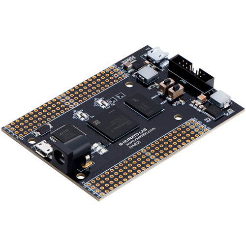
Tagus A7 PCI Express Development Board
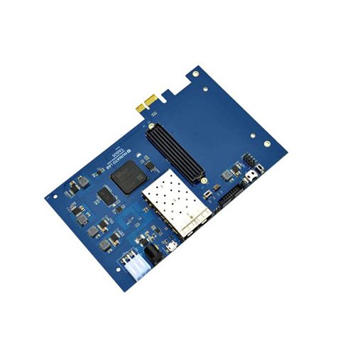

Tagus A7 PCI Express Development Board Specification
- Flame Resistance Level
- UL94 V-0
- Min. Line Spacing
- 0.13mm
- Test
- 100% E-test
- Board Type
- PCI Express Development
- Hole Size
- 0.2mm (min)
- Voltage Endurance
- 50V DC
- Silkscreen
- White
- Soldermask
- Green
- Min. Line Width
- 0.13mm
- Impedance
- Controlled, 50
- Insulation Resistance
- >500 M
- Product Type
- FPGA Development board
- Base Material
- FR4
- Surface Finish
- ENIG (Electroless Nickel Immersion Gold)
- Copper Thickness
- 1oz
- Board Thickness
- 1.6mm
- Color
- Green
- Panel Size
- 140mm x 95mm
- Sensor Switch
- No
- Electrical Components
- Includes Artix-7 FPGA, PCI Express Edge Connector, DDR3 Memory
- Number Of Layers
- 4
- Memory
- 512MB DDR3 SDRAM
- Button/Switches
- 4 user push-button switches, 4 DIP switches
- Expansion Interface
- Pmod, FMC Standard Compatible
- Programming Interface
- JTAG
- RoHS Compliance
- Yes, Lead Free
- Power Supply
- PCIe Bus-powered or External 5V Input
- Connectivity
- PCI Express x1 Gen2 Interface
- PCB Finish
- Glossy
- Operating Temperature Range
- 0C to +70C
- LED Indicators
- 8 user LEDs
- Mounting Holes
- M3, 4 corners
- On-board Oscillator
- 50MHz
- FPGA Chip
- Xilinx Artix-7 (XC7A35T)
Tagus A7 PCI Express Development Board Trade Information
- Minimum Order Quantity
- 1 Unit
- Supply Ability
- 10 Units Per Day
- Delivery Time
- 1-4 Days
About Tagus A7 PCI Express Development Board
Features
- FPGA: AMD Artix-7 XC7A200T in -2 FBG484I package
- 1 lane PCIe Gen2.0(5.0GT/s)
- DDR3: 2Gb DDR3 (MT41J128M16HA-125:K or equivalent)
- 128 Mb QSPI flash memory (N25Q128A13ESE40E) for Configuration and optional data storage
- USB to UART serial converter
- 1 x 100MHz CMOS oscillator
- Maximum 68 IOs for user-defined purposes on ANSI/VITA 57.1 Standard-compliant FMC LPC connector
- 1x GTP lanes up to 6.6Gbps on ANSI/VITA 57.1 Standard-compliant FMC LPC connector
- 1 RGB LED for custom use
- 1x Trusted Platform Module (ATXXXXXX )
- Dual SFP Cages
- MicroSD adapter for bulk data storage
- Onboard voltage regulators for single-power rail operation
- Can be powered from a PCIe slot or an external power supply
- JTAG header for programming and debugging
- All differential pairs are length matched on the board
Applications
- Parallel Processing and Accelerators
- Product Prototype Development
- Development and Testing of custom-embedded processors
- Signal Processing
- Communication Device Development
- Data Acquisition
- Educational tool for Schools and Universities
Versatile FPGA Development Platform
Experience flexible and scalable development with the Tagus A7 PCI Express Board, centered on the powerful Xilinx Artix-7 (XC7A35T) FPGA. Its combination of high-speed memory, PCIe Gen2 connectivity, and extensive user interfaces makes it suitable for a broad range of applications, from learning environments to industrial prototyping.
Seamless Expansion and Connectivity
Equipped with Pmod and FMC standard interfaces, the board allows straightforward expansion for custom peripherals or testing modules. The onboard DDR3 memory and PCI Express edge connector ensure high-speed data communication for demanding projects, all powered efficiently through PCIe or an external 5V input.
FAQ's of Tagus A7 PCI Express Development Board:
Q: How can I program the Tagus A7 PCI Express Development Board?
A: The board is easily programmed via the onboard JTAG interface, compatible with standard Xilinx programming tools such as Vivado design suite. Simply connect your programming cable to the JTAG header and follow your preferred development workflow.Q: What are the power supply options for this development board?
A: The board can be powered directly from the PCI Express bus or using an external 5V input. This dual power option offers flexibility for development and deployment in diverse environments.Q: When is it beneficial to use the PCI Express x1 Gen2 interface on this board?
A: Employ the PCIe x1 Gen2 interface whenever you need high-speed data transfer between the FPGA board and a host system, such as for real-time data processing or interfacing with PC-based applications.Q: Where can the Tagus A7 board be mounted?
A: With M3 mounting holes at all four corners, the board can be securely installed in custom enclosures, development racks, or test benches, facilitating safe and stable project setups.Q: What process is involved in interfacing additional modules via the expansion interface?
A: You can utilize the Pmod and FMC standard compatible headers to connect expansion modules, such as sensors or custom boards. Simply plug compatible modules into the respective headers, configure your FPGA design, and begin utilizing the extended features.Q: How can I monitor or debug my design with the onboard features?
A: The board provides 8 user-controlled LEDs, 4 push-buttons, and 4 DIP switches, which you can assign within your FPGA design as status indicators or user-input devices for rapid debugging and prototyping.Q: What are the benefits of the board's RoHS compliance and quality construction?
A: Being RoHS compliant and built with lead-free processes on a 4-layer FR4 PCB with ENIG surface finish, the board ensures durability, environmental safety, and reliable signal integrity, ideal for critical prototype and production applications.Tell us about your requirement

Price:
Quantity
Select Unit
- 50
- 100
- 200
- 250
- 500
- 1000+
Additional detail
Mobile number
Email

More Products in FPGA Boards Category
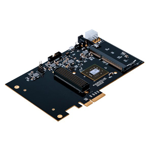
Nereid K7 PCI Express FPGA Development Board
Price 110000 INR / Unit
Minimum Order Quantity : 1 Unit
Board Type : Rigid
Product Type : FPGA Development board
Panel Size : Standard PCIe form factor
Number Of Layers : Other, 6 Layers
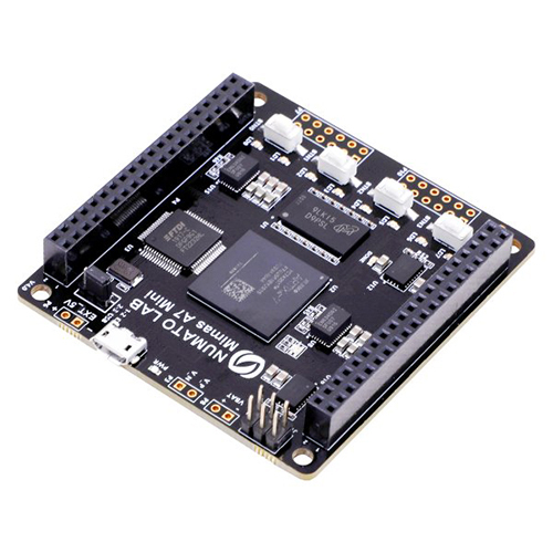
Mimas A7 Mini FPGA Development Board
Price 16500 INR / Unit
Minimum Order Quantity : 1 Unit
Board Type : Rigid
Product Type : FPGA Development board
Panel Size : 70 mm x 40 mm
Number Of Layers : Other, 4
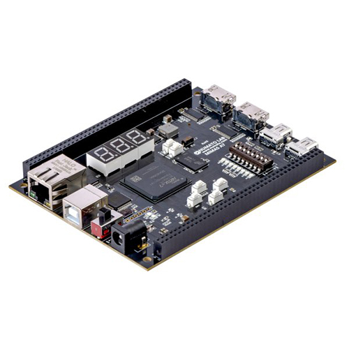
Mimas A7 FPGA Development Board
Price 25300 INR / Unit
Minimum Order Quantity : 1 Unit
Board Type : Other, FR4 PCB
Product Type : FPGA Development board
Panel Size : Approximately 100 mm x 70 mm
Number Of Layers : Other, 4Layer PCB
Narvi S7 FPGA Module
Price 22000 INR / Unit
Minimum Order Quantity : 1 Unit
Board Type : Rigid
Product Type : FPGA Development board
Panel Size : 114mm x 64mm
Number Of Layers : Other, 4
Our Products


H No 2-3-54, Co-Operative Bank Colony, Road No. 6, Nogole,Hyderabad - 500068, Telangana, India

Mr Suneel
Mobile :08045812175
 Send Inquiry
 Send SMS
 Call Me Free
Developed and Managed by Infocom Network Private Limited.
