Call us now :08045812175
Mimas A7 FPGA Development Board
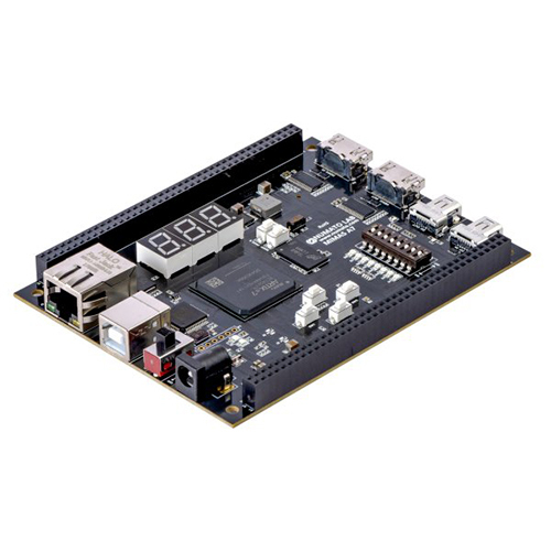

Mimas A7 FPGA Development Board Specification
- Test
- 100% Electrical Testing
- Impedance
- Controlled Impedance Routing
- Min. Line Spacing
- 0.1 mm
- Voltage Endurance
- 250V AC
- Soldermask
- Green
- Silkscreen
- White
- Min. Line Width
- 0.1 mm
- Flame Resistance Level
- UL94-V0
- Insulation Resistance
- >10^12 Ohm
- Hole Size
- 0.3 mm (min)
- Board Type
- FR4 PCB
- Product Type
- FPGA Development board
- Base Material
- FR4 Epoxy Glass
- Surface Finish
- ENIG (Electroless Nickel Immersion Gold)
- Copper Thickness
- 1 oz (35 m)
- Board Thickness
- 1.6 mm
- Color
- Green
- Panel Size
- Approximately 100 mm x 70 mm
- Sensor Switch
- Tactile Push Buttons
- Electrical Components
- Xilinx Artix-7 (XC7A35T) FPGA, 512Mb DDR3 SDRAM, Onboard configurations switches, LEDs, USB-UART, USB-JTAG, Micro SD card slot, SPI Flash
- Number Of Layers
- 4-Layer PCB
- Mounting Holes
- 4 at corners
- Onboard Memory
- 512Mb DDR3 SDRAM
- Input Supply Voltage
- 5V (USB powered)
- Power Supply
- Micro-USB powered, compatible with USB chargers
- Supported Voltage
- 3.3V I/O, 5V Power
- Onboard LEDs
- 8 user LEDs
- Compatible Software
- Xilinx Vivado Design Suite
- FPGA Device
- Xilinx Artix-7 XC7A35T
- Switches
- 8 DIP switches
- USB Interface
- Micro-USB, USB-UART
- Expansion Connectors
- Pmod compatible headers
- Programming Interface
- Onboard JTAG Programmer
- Clock Source
- 100 MHz onboard oscillator
- Configuration
- MicroSD Card slot, USB JTAG, SPI Flash
- I/O Pins
- 90 I/O pins
- Push Buttons
- 5 user push buttons
- Operating Temperature
- 0 - 70C
Mimas A7 FPGA Development Board Trade Information
- Minimum Order Quantity
- 1 Unit
- Supply Ability
- 10 Units Per Day
- Delivery Time
- 1-4 Days
About Mimas A7 FPGA Development Board
Features
- Device: AMD Artix 7 FPGA (XC7A50T-1FGG484C)
- DDR3: 2Gb DDR3 (MT41J128M16HA-125 or equivalent)
- FTDI FT2232H based host interface
- Built-in programming interface. No expensive JTAG adapters needed for programming the board
- Gigabit Ethernet
- HDMI IN/OUT interfaces
- High-Speed Serial Interface (GTP) available on mini DisplayPort connectors
- Onboard 128Mb flash memory for FPGA configuration storage and custom user data storage
- 100MHz CMOS oscillator
- Micro SD card slot for memory expansion
- Seven Segment Display and switches for easy learning, prototyping and debugging
- FPGA configuration via JTAG and USB
- 80 IOs (40 professionally length matched Differential Pairs) for user-defined purposes
Applications
- Product Prototype Development
- Accelerated computing integration
- Development and testing of custom embedded processors
- Signal Processing
- Communication device development
- Educational tool for Schools and Universities
- Video processing
Powerful and Flexible FPGA Platform
Mimas A7 is built around the Xilinx Artix-7 XC7A35T FPGA, coupled with 512Mb DDR3 SDRAM, supporting high-speed data processing and storage. With 90 user I/O pins, expansion headers, and standard voltage levels (3.3V I/O, 5V power), it excels in diverse digital design applications. The high-quality four-layer PCB ensures reliable performance, while integrated configuration interfaces enable rapid prototyping and seamless workflow.
User-Friendly Connectivity and Expansion
This board offers flexible connection options with Pmod headers, a Micro-USB interface, and MicroSD slot, guaranteeing easy addition of peripherals and modules. Onboard configuration support via USB JTAG and SPI Flash simplifies programming, while accessible LEDs, switches, and buttons facilitate interactive projects and debugging.
Compatibility and Development Tools
Mimas A7 shines with its compatibility with Xilinx Vivado Design Suite, making development, simulation, and synthesis efficient and straightforward. Its user-friendly features and comprehensive documentation support rapid experimentation, making it ideal for students, hobbyists, and engineers working in embedded systems or digital logic design.
FAQs of Mimas A7 FPGA Development Board:
Q: How do I program the Mimas A7 FPGA Development Board?
A: You can program the Mimas A7 board using the onboard USB JTAG programmer, which is compatible with Xilinx Vivado Design Suite. Additionally, configuration via SPI Flash or a MicroSD card slot is supported for flexible design deployment.Q: What advantages does the onboard 512Mb DDR3 SDRAM provide?
A: The 512Mb DDR3 SDRAM enables fast and efficient memory access, allowing for complex data processing, buffering, and storage tasks, which is crucial for demanding FPGA applications such as image processing or signal analysis.Q: When should I use the Pmod compatible headers?
A: Use the Pmod compatible headers when you wish to connect additional modules, such as sensors, displays, or communications interfaces, to expand the boards capabilities or to prototype custom peripherals quickly.Q: Where can I power the board from and what are the supply requirements?
A: The board is powered via a Micro-USB port, making it compatible with standard USB chargers, computers, or power banks. It operates reliably on a 5V input and supports 3.3V logic levels on the I/O pins.Q: What is the process of configuring the FPGA using the MicroSD card?
A: To configure the FPGA via the MicroSD card, place your bitstream file onto a compatible MicroSD card, insert it into the onboard slot, and set the configuration switches as detailed in the user guide. The board will automatically load the design at power-up.Q: How can onboard LEDs, switches, and push buttons enhance my project?
A: The eight user LEDs, five push buttons, and eight DIP switches provide interactive inputs and visual outputs, useful for interfacing, debugging, or prototyping user-controlled operations during FPGA development.Q: What are the benefits of the boards four-layer FR4 PCB and ENIG surface finish?
A: The four-layer FR4 PCB ensures low electrical noise and robust signal integrity, while the ENIG surface finish enhances solderability, reliability, and longevity of the board, making it suitable for both professional and educational use.Tell us about your requirement

Price:
Quantity
Select Unit
- 50
- 100
- 200
- 250
- 500
- 1000+
Additional detail
Mobile number
Email

More Products in FPGA Boards Category
Narvi S7 FPGA Module
Price 22000 INR / Unit
Minimum Order Quantity : 1 Unit
Product Type : FPGA Development board
Board Type : Rigid
Voltage Endurance : >1000V
Base Material : FR4
Callisto K7 USB 3.1 FPGA Module
Price 104500 INR / Unit
Minimum Order Quantity : 1 Unit
Product Type : FPGA Development board
Board Type : Rigid
Voltage Endurance : >1000V
Base Material : Other, FR4
Neso A7 FPGA Development Board
Price 35200 INR / Unit
Minimum Order Quantity : 1 Unit
Product Type : FPGA Development board
Board Type : Other, SMD, Through Hole
Voltage Endurance : 50V DC
Base Material : FR4

Callisto S6 USB 3.1 FPGA Module
Price 71280 INR / Unit
Minimum Order Quantity : 1 Unit
Product Type : FPGA Development board
Board Type : Other, Module
Voltage Endurance : 50 VDC
Base Material : FR4
Our Products


H No 2-3-54, Co-Operative Bank Colony, Road No. 6, Nogole,Hyderabad - 500068, Telangana, India

Mr Suneel
Mobile :08045812175
 Send Inquiry
 Send SMS
 Call Me Free
Developed and Managed by Infocom Network Private Limited.
