
Call us now :08045812175
 Send Inquiry
FPGA Development Board Neso A7
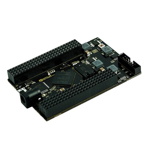

FPGA Development Board Neso A7 Specification
- Silkscreen
- White
- Insulation Resistance
- >500 M
- Min. Line Spacing
- 6 mil
- Min. Line Width
- 6 mil
- Flame Resistance Level
- 94V-0
- Board Type
- SMD, Through Hole
- Hole Size
- 0.3 mm (min)
- Test
- Other
- Voltage Endurance
- 50V DC
- Soldermask
- Green
- Impedance
- Controlled
- Product Type
- FPGA Development board
- Base Material
- FR4
- Surface Finish
- Other
- Copper Thickness
- 1 oz
- Board Thickness
- 1.6 mm
- Color
- Green
- Panel Size
- Standard
- Sensor Switch
- Push Button, DIP Switches
- Electrical Components
- FPGA, Voltage Regulator, Connectors, LEDs, Oscillator
- Number Of Layers
- 4
- FPGA Device
- Xilinx Artix-7 (XC7A35T-1CPG236C)
- Clock Source
- 100 MHz onboard crystal oscillator
- Power Supply
- External 5V, USB powered
- Dimensions
- ~120mm x 80mm
- Programming Interface
- JTAG, USB
- On-board Memory
- 256Mb SPI Flash, 64MB DDR3 SDRAM
- I/O Pins
- 80+ (through PMOD and GPIO headers)
- On-board Peripherals
- 4x LEDs, 4x Push Buttons, 4x DIP Switch, Buzzer
- Interfaces
- USB-UART, USB-JTAG, HDMI, VGA, Audio Out, Ethernet, MicroSD slot, PS/2
- Operating Temperature
- 0C to +70C
FPGA Development Board Neso A7 Trade Information
- Minimum Order Quantity
- 1 Unit
- Supply Ability
- 10 Units Per Day
- Delivery Time
- Days
About FPGA Development Board Neso A7
Features
- FPGA: XC7A100T in CSG324 package (XC7A100T-2CSG324C)
- DDR3: 2Gb DDR3(MT41J128M16JT-125:K)
- Flash memory: 128 Mb SPI flash memory (N25Q128A13ESE40E / IS25LP128F " JBLE)
- 100MHz CMOS oscillator
- High-Speed USB 2.0 interface for Onboard flash programming.
- Revision V1: FT2232H Channel A is dedicated to SPI Flash /JTAG Programming. Channel B can be used for custom applications.
- Revision V2: FT2232H Channel B is dedicated to SPI Flash /JTAG Programming. Channel A can be used for custom applications.
- Onboard voltage regulators for single power rail operation
- FPGA configuration via JTAG and USB
- Compact form factor FPGA Module
- Maximum IOs for user-defined purposes
- FPGA " 140 IOs
- FT2232H " 8 IOs
Versatile Connectivity and Expansion
With over 80 I/O pins accessible through PMOD and GPIO headers, Neso A7 allows seamless interfacing with a wide array of external modules. The board features various interfaces like USB-UART, HDMI, and Ethernet, offering compatibility with modern communication protocols. This flexibility makes it suitable for sophisticated design and testing environments.
Comprehensive On-board Memory Support
Equipped with 256Mb SPI Flash and 64MB DDR3 SDRAM, the Neso A7 provides robust memory capabilities for large-scale designs and real-time applications. This ample memory enables smooth operation of complex algorithms and enhances design performance, making the board capable of handling demanding use-cases.
Reliable and User-Friendly Design
Built with durable FR4 material and a standard panel size, the Neso A7 offers a compact yet sturdy build. On-board peripherals such as LEDs, switches, and buzzers, combined with 100% electrical testing and high insulation resistance, ensure reliable and safe operation. Its green, lead-free surface is complemented by a clear white silkscreen for easy component identification.
FAQ's of Neso A7 FPGA Development Board:
Q: How do I program the Neso A7 FPGA Development Board?
A: The Neso A7 can be programmed using the USB-JTAG or standard JTAG interface. Support for standard development tools provided by Xilinx enables you to configure and debug the onboard Artix-7 FPGA with ease. USB programming also simplifies setup for beginners.Q: What types of projects benefit from using the Neso A7 board?
A: The Neso A7 is well-suited for digital signal processing, embedded system design, communication protocol development, image and video processing, and hardware prototyping. Educational institutions, industrial researchers, and electronics enthusiasts leverage its versatility for a variety of applications.Q: When should I use the external 5V power supply instead of USB power?
A: An external 5V power supply should be used when your application requires higher current for peripherals, or when USB power is not sufficient to meet your system's needs. For low power designs or development tasks, USB power is typically adequate.Q: Where are the I/O pins accessible on the Neso A7 board?
A: I/O pins are accessible via the PMOD and GPIO headers located on the board. These headers facilitate easy connection to sensors, displays, and other external devices, expanding the board's functionality to suit a wide range of hardware experiments.Q: What is the process for updating the configuration on the FPGA?
A: To update the FPGA configuration, connect your board using USB-JTAG or JTAG, then use the Xilinx Vivado or iMPACT tool to load your bitstream file to the FPGA. The 256Mb SPI Flash also allows for non-volatile storage of configurations, supporting automatic loading on power-up.Q: How can I utilize the onboard peripherals for prototyping?
A: The board features 4 LEDs, 4 push buttons, 4 DIP switches, and a buzzer. These can be easily accessed and controlled via the FPGA, enabling quick implementation, validation, and demonstration of user interfaces or logic designs, making prototyping intuitive and interactive.Q: What are the key benefits of the Neso A7's hardware and construction standards?
A: The board uses a 4-layer FR4 base, 1 oz copper thickness, and is 94V-0 flame resistant. With controlled impedance and rigorous 100% electrical testing, it offers excellent signal integrity, durability, and reliability, ensuring optimal performance for critical applications.Tell us about your requirement

Price:
Quantity
Select Unit
- 50
- 100
- 200
- 250
- 500
- 1000+
Additional detail
Mobile number
Email

More Products in FPGA Boards Category
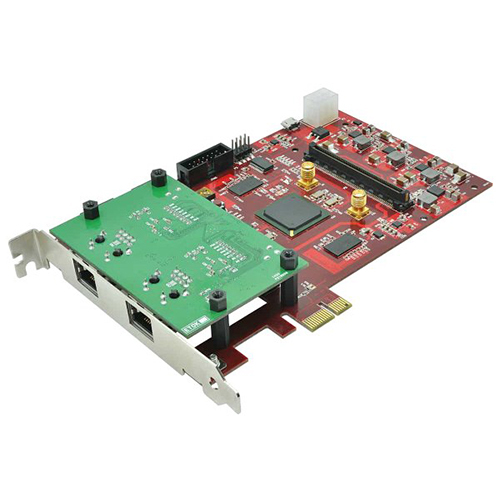
Galatea PCI Express S6 FPGA Development Board
Price 30030 INR / Unit
Minimum Order Quantity : 1 Unit
Copper Thickness : 1 oz
Min. Line Spacing : 6 mil
Insulation Resistance : >10^12
Soldermask : Blue
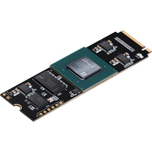
Aller A7 FPGA Board with M.2 Interface
Price 55000 INR / Unit
Minimum Order Quantity : 1 Unit
Copper Thickness : 1 oz
Min. Line Spacing : 6 mil
Insulation Resistance : >=10^12
Soldermask : Green
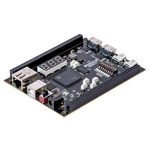
FPGA Development Board
Price 70.0 INR / Unit
Minimum Order Quantity : 1 Unit
Copper Thickness : 1 oz (35 m)
Min. Line Spacing : 0.1 mm
Insulation Resistance : >10^12 Ohm
Soldermask : Green
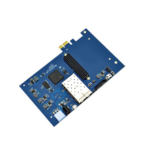
PCI Express
Price 66000 INR / Unit
Minimum Order Quantity : 1 Unit
Copper Thickness : 1oz
Min. Line Spacing : 0.13mm
Insulation Resistance : >500 M
Soldermask : Green


 Send Inquiry
Our Products


H No 2-3-54, Co-Operative Bank Colony, Road No. 6, Nogole,Hyderabad - 500068, Telangana, India

Mr Suneel
Mobile :08045812175
 Send Inquiry
 Send SMS
Developed and Managed by Infocom Network Private Limited.
